Summary
t
Figures

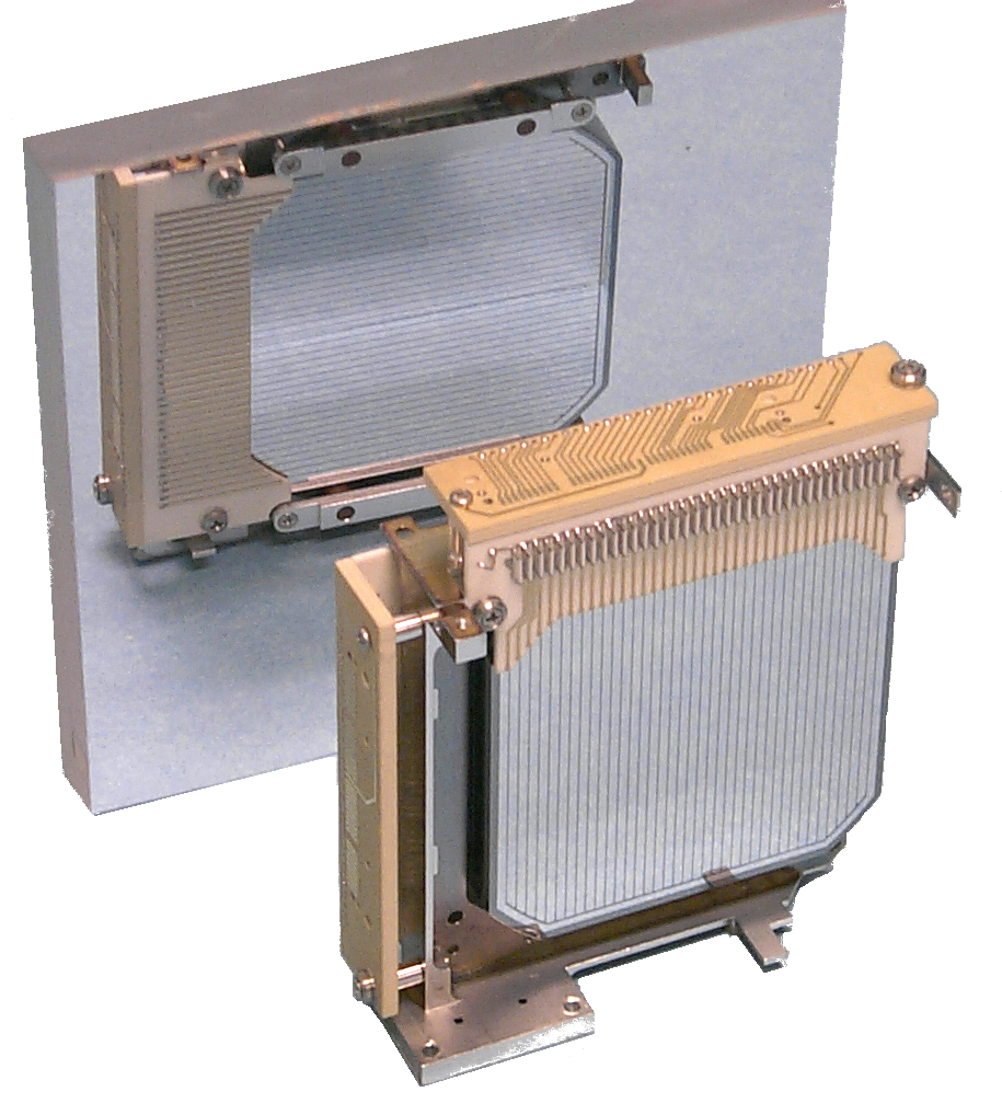
The image shows a piece of laboratory equipment, specifically an ultraviolet (UV) spectrophotometer. This instrument is used to measure the absorbance of light at different wavelengths in the ultraviolet range. It’s designed to analyze the molecular structure of chemicals, helping scientists identify and quantify different components in a sample.
The UV spectrophotometer has two main parts visible in the image:
1. **Sample Holder**: This is where you place your sample that needs to be analyzed. The holder usually contains a transparent glass or quartz plate through which the light passes. The sample holder appears to have a clear window, allowing for direct observation of the sample.
2. **Photodetector**: This is the device that measures the intensity of light passing through the sample holder. It converts the light absorbance into an electrical signal proportional to the concentration of the sample’s absorbing species.
The equipment has a control panel or interface on the right, which likely includes buttons and displays for operating the instrument, setting wavelengths, and displaying the results. The image shows only two sides of the photodetector, so you would typically see at least three sides (front, left, and right) to get a complete view of the device’s construction.
The UV spectrophotometer is an important tool in chemistry, biology, and materials science research. It can be used for a wide range of applications such as determining the purity of water or other liquids, identifying and quantifying components in chemical mixtures, studying the effects of pH on the spectrum of absorption peaks, and much more.

This image appears to be a scientific or technical diagram, possibly from a publication in the field of physics, electronics, or related sciences. The diagram is schematic and not photographic, which suggests it’s meant to represent an experiment or a conceptual model.
The diagram shows a setup with various components labeled as follows:
– HV (High Voltage): This likely represents the high voltage source that powers the device in question.
– Electrode: These are typically conductive materials that facilitate electrical flow, possibly used to generate or measure an electric field.
– Photon: This term is often associated with a particle of light, but it could also refer to an electron (e-) or another charged particle.
– LV (Low Voltage): This likely represents the lower voltage side of the circuit or setup.
– Vq: This could represent a voltage difference or gradient between two points within the system.
The lines with arrows point from the HV to the electrode, indicating that the high voltage is applied across the electrode. The presence of electrons (e-) suggests that this might be an electron beam or a setup involving electron flow and electric fields.
Below the diagram, there’s a table with some form of data or results. The table has two columns:
– Q/V (Coulomb per Volt)
– Free Electrons / holes
The first row shows “0” for both columns, which could indicate that at zero voltage, there are no free electrons or holes. Each subsequent row seems to increment the voltage (Q/V), and there is an increase in the number of free electrons and holes. This trend suggests a relationship between the applied electric field and the number of charge carriers generated or detected.
The specific context of this diagram, such as its relevance to physics, materials science, or engineering, would require further information or understanding of the text accompanying it, which is not fully visible in the image provided.

This image appears to be a schematic representation of an electronics or signal processing concept, possibly from an academic paper or presentation slide. Here’s a breakdown of the components and elements present in the figure:
1. **Collection Signal (Red line with black squares)**: This represents a time series of data or a signal that is being collected at regular intervals. The x-axis indicates time, suggesting this could be a sequence of measurements taken over time.
2. **Electron Collection (Symbols Q and E)**: These symbols typically represent charge and energy, respectively. They indicate the quantities of these properties that are being measured or analyzed in real-time.
3. **Hole Collection Signal (Blue line with green squares)**: This signal seems to be related to holes in semiconductor physics, which could be referring to electron holes if this is a circuit diagram. Electron holes are regions of positive charge, and this signal might represent the collection or movement of these holes over time.
4. **Electron (Red circle with black line)**: The red circle with a black line indicates an electron, which is a negatively charged particle that can move through semiconductors as well as conduct electricity.
5. **Temporal Correlation (Black line with a square symbol at the beginning and end)**: This represents the correlation between two temporal signals over time. It suggests that there is some relationship or pattern in the signals at different points in time, which could be significant for understanding the system’s behavior.
6. **Charge (Q) and Energy (E)**: These are traditional terms from physics and chemistry used to describe the properties of particles. Charge can be positive or negative and is measured in coulombs (C). Energy is typically measured in Joules (J).
7. **Time (x-axis)**: This axis shows the time at which each measurement is taken or processed. The x-axis spans from 0 to t_max, where t_max likely represents the end of the data collection period.
8. **Threshold (dotted line with a square symbol)**: This threshold might represent a certain condition or level that has been set for analysis. If the measurement exceeds this threshold, some action or event occurs.
9. **Charge (Q) vs Energy (E)**: The y-axis represents the relationship between charge and energy in the system being analyzed.
10. **Hole (Green circle with a black line)**: This indicates the presence of a hole, which is a region where an electron could appear and move through semiconductors, such as in p-type semiconductors.
The overall context suggests that this figure is related to a study involving electronic properties, possibly within the field of condensed matter physics or semiconductor material science. The temporal correlation between the electron’s movement and energy changes could be of interest for understanding how the system operates over time.
